- 您现在的位置:买卖IC网 > Sheet目录331 > IR21141SSPBF (International Rectifier)IC DRVR HALF BRIDGE 600V 24-SSOP
IR2114/IR2214SSPbF
? Charge required by the internal level shifters
2 Sizing Tips
2.1 Bootstrap Supply
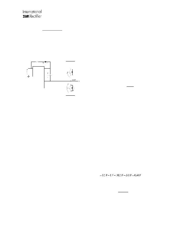
The V BS voltage provides the supply to the high side
driver circuitry of the gate driver. This supply sits on top
of the V S voltage and so it must be floating. The
bootstrap method is used to generate the V BS supply
and can be used with any of the IR211(4,41)/
IR221(4,41) drivers. The bootstrap supply is formed by
a diode and a capacitor as connected in Fig. 19.
( Q LS ); typical 20 nC,
? Bootstrap capacitor leakage current ( I LK_CAP ),
? High side on time ( T HON ).
I LK_CAP is only relevant when using an electrolytic
capacitor and can be ignored if other types of
capacitors are used. It is strongly recommend using at
least one low ESR ceramic capacitor (paralleling
electrolytic and low ESR ceramic may result in an
efficient solution).
bootstrap
resistor
R boot
bootstrap
diode
V F
DC+
Then we have:
Q TOT = Q G + Q LS + ( I LK _ GE + I QBS +
V CC
VCC
VB
HOP
HON
VS
V BS
bootstrap
capacitor
V GE
I LOAD
motor
+ I LK + I LK _ DIODE + I LK _ CAP + I DS ? ) ? T HON
The minimum size of bootstrap capacitor is:
SSDH
V CEon
V FP
C BOOT min =
Q TOT
? V BS
COM
Figure 19: Bootstrap Supply Schematic
An example follows using IR2214SS or IR22141SS:
a) using a 25 A @ 125 °C 1200 V IGBT
(IRGP30B120KD):
This method has the advantage of being simple and low
cost but may force some limitations on duty-cycle and
on-time since they are limited by the requirement to
refresh the charge in the bootstrap capacitor. Proper
capacitor choice can reduce drastically these
limitations.
2.2 Bootstrap Capacitor Sizing
To size the bootstrap capacitor, the first step is to
establish the minimum voltage drop ( ? V BS ) that we
?
?
?
?
?
?
?
?
?
I QBS = 800 μA (datasheet IR2214);
I LK = 50 μA (see Static Electrical Characteristics);
Q LS = 20 nC
Q G = 160 nC (datasheet IRGP30B120KD);
I LK_GE = 100 nA (datasheet IRGP30B120KD);
I LK_DIODE = 100 μA (reverse recovery <100 ns);
I LK_CAP = 0 (neglected for ceramic capacitor);
I DS- = 150 μA (see Static Electrical Characteristics);
T HON = 100 μs.
have to guarantee when the high side IGBT is on.
And:
If V GEmin is the minimum gate emitter voltage we want
to maintain, the voltage drop must be:
? V BS ≤ V CC ? V F ? V GE min ? V CEon
?
?
?
?
V CC = 15 V
V F = 1 V
V CEonmax = 3.1 V
V GEmin = 10.5 V
under the condition,
V GE min > V BSUV ?
where V CC is the IC voltage supply, V F is bootstrap
diode forward voltage, V CEon is emitter-collector voltage
of low side IGBT, and V BSUV- is the high-side supply
undervoltage negative going threshold.
the maximum voltage drop ? V BS becomes
? V BS ≤ V CC ? V F ? V GE min ? V CEon =
And the bootstrap capacitor is:
Now we must consider the
influencing
factors
contributing V BS to decrease:
? IGBT turn on required gate charge ( Q G ),
C BOOT ≥
290 nC
0 . 4 V
= 725 nF
? IGBT gate-source leakage current ( I LK_GE ),
? Floating section quiescent current ( I QBS ),
? Floating section leakage current ( I LK ),
? Bootstrap diode leakage current ( I LK_DIODE ),
? Desat diode bias when on ( I DS ),
www.irf.com
16
NOTICE: V CC has been chosen to be 15 V. Some
IGBTs may require a higher supply to work correctly
with the bootstrap technique. Also V CC variations
must be accounted in the above formulas.
? 2009 International Rectifier
发布紧急采购,3分钟左右您将得到回复。
相关PDF资料
IR2118PBF
IC MOSFET DRIVER HIGH-SIDE 8-DIP
IR2121PBF
IC MOSFET DRIVER LOW SIDE 8DIP
IR2122
IC MOSFET DRIVER HIGH-SIDE 8-DIP
IR2125PBF
IC MOSFET DRIVER LIMITING 8-DIP
IR21271PBF
IC DRIVER 600V 200/420MA 8-DIP
IR2132JTRPBF
IC DRIVER BRIDGE 3-PHASE 44-PLCC
IR2132JTR
IC DRIVER BRIDGE 3-PHASE 44-PLCC
IR21363JPBF
IC DRIVER 3-PHASE 44-PLCC
相关代理商/技术参数
IR21141SSPBF_09
制造商:IRF 制造商全称:International Rectifier 功能描述:HALF-BRIDGE GATE DRIVER IC
IR21141SSTRPBF
功能描述:功率驱动器IC 600V Hlf Brdg Drvr IC for Pwr Swtch App RoHS:否 制造商:Micrel 产品:MOSFET Gate Drivers 类型:Low Cost High or Low Side MOSFET Driver 上升时间: 下降时间: 电源电压-最大:30 V 电源电压-最小:2.75 V 电源电流: 最大功率耗散: 最大工作温度:+ 85 C 安装风格:SMD/SMT 封装 / 箱体:SOIC-8 封装:Tube
IR2114SS
功能描述:IC DRIVER HALF-BRIDGE 24-SSOP RoHS:否 类别:集成电路 (IC) >> PMIC - MOSFET,电桥驱动器 - 外部开关 系列:- 标准包装:50 系列:- 配置:高端 输入类型:非反相 延迟时间:200ns 电流 - 峰:250mA 配置数:1 输出数:1 高端电压 - 最大(自引导启动):600V 电源电压:12 V ~ 20 V 工作温度:-40°C ~ 125°C 安装类型:通孔 封装/外壳:8-DIP(0.300",7.62mm) 供应商设备封装:8-DIP 包装:管件 其它名称:*IR2127
IR2114SSPBF
功能描述:功率驱动器IC 600V HALF BRDG DRVR IC RoHS:否 制造商:Micrel 产品:MOSFET Gate Drivers 类型:Low Cost High or Low Side MOSFET Driver 上升时间: 下降时间: 电源电压-最大:30 V 电源电压-最小:2.75 V 电源电流: 最大功率耗散: 最大工作温度:+ 85 C 安装风格:SMD/SMT 封装 / 箱体:SOIC-8 封装:Tube
IR2114SSPBF
制造商:International Rectifier 功能描述:Driver IC
IR2114SSTRPBF
功能描述:功率驱动器IC 600V Hlf Brdg Drvr IC for Pwr Swtch App RoHS:否 制造商:Micrel 产品:MOSFET Gate Drivers 类型:Low Cost High or Low Side MOSFET Driver 上升时间: 下降时间: 电源电压-最大:30 V 电源电压-最小:2.75 V 电源电流: 最大功率耗散: 最大工作温度:+ 85 C 安装风格:SMD/SMT 封装 / 箱体:SOIC-8 封装:Tube
IR2117
功能描述:IC MOSFET DRIVER SGL-CH 8-DIP RoHS:否 类别:集成电路 (IC) >> PMIC - MOSFET,电桥驱动器 - 外部开关 系列:- 标准包装:50 系列:- 配置:高端 输入类型:非反相 延迟时间:200ns 电流 - 峰:250mA 配置数:1 输出数:1 高端电压 - 最大(自引导启动):600V 电源电压:12 V ~ 20 V 工作温度:-40°C ~ 125°C 安装类型:通孔 封装/外壳:8-DIP(0.300",7.62mm) 供应商设备封装:8-DIP 包装:管件 其它名称:*IR2127
IR2117PBF
功能描述:功率驱动器IC 1 HI SIDE DRVR NONINVERTING INPUT RoHS:否 制造商:Micrel 产品:MOSFET Gate Drivers 类型:Low Cost High or Low Side MOSFET Driver 上升时间: 下降时间: 电源电压-最大:30 V 电源电压-最小:2.75 V 电源电流: 最大功率耗散: 最大工作温度:+ 85 C 安装风格:SMD/SMT 封装 / 箱体:SOIC-8 封装:Tube
